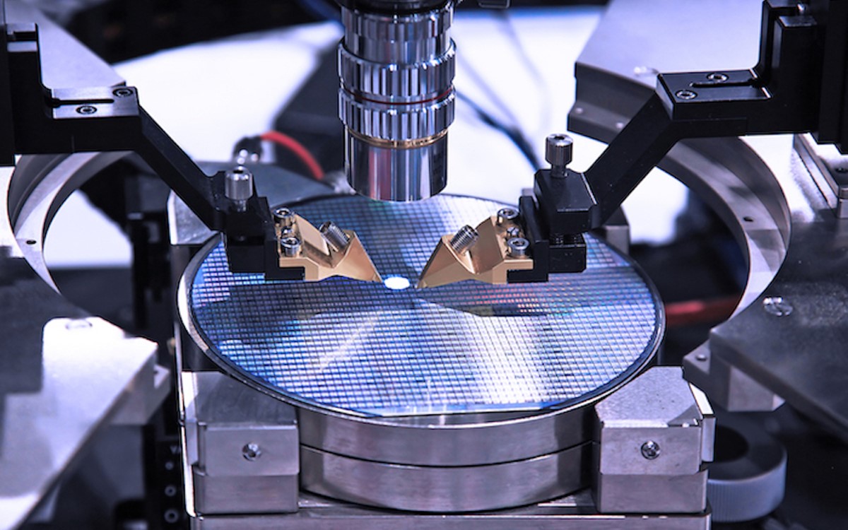
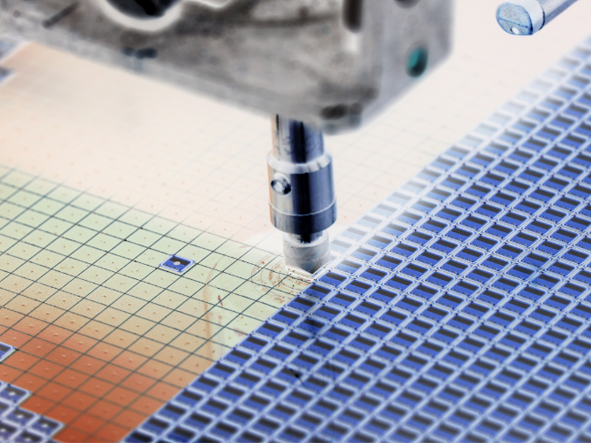
Photoresists have been used for a long time in processes such as photolithography and photoengraving. This has become a crucial process in the electronics industry, helping to form a patterned coating on a surface, such as a circuit board, where it can work with a developer during the etching process to create accurate circuits and electrical pathways.
There are different types of photoresists available, and a positive photoresist is a light-sensitive material used in photolithography to help create the intricate patterns which can be found in electronic circuits. Positive photoresists are used for their many unique properties and applications.

Chemical properties
There are several different chemicals involved in creating positive photoresists. The three main components are resin, a photosensitive agent, and a solvent. The resin is used for adhesion, solubility and resolution, whilst the photosensitive agent is a photo-acid generator that releases acid when exposed to UV light in order to alter the solubility of the resin. Typical photosensitive agents include onium salts, sulfonium salts and diazonaphthoquinones which are dissolved in the solvent. This helps to produce a homogeneous solution that can then be spin-coated onto a substrate. It is important to note that the precise makeup of a positive photoresist will change depending on the resist and the desired characteristics for the finished pattern. Each chemical substance has its special characteristics and so it is important to choose the right ones for each photoresist to create the desired effect.
Physical properties
A typical photoresist has several important properties which will need to be selected based on the individual process it is to be used for, with the main ones including resolution capability, process dose and focused latitudes required for curing, as well as their resistance to reactive ion etching. It is also important to pay attention to their sensitivity, their compatibility with tetramethylammonium hydroxide, their adhesion, environmental stability and how long they last.
The high resolution of the positive photoresist gives the ability to differ the neighbouring features on the substrate, whilst the contrast is the difference from the exposed portion to the unexposed portion. The sensitivity of the photoresist will have certain minimum energy levels which are required to generate a well-defined feature, and the viscosity measures the internal friction of a fluid and how easily it will flow. The adherence is the strength between the photoresist and substrate, whilst the etching resistance is the ability to resist the high temperature, pH environment or the ion bombardment post-modification.
Process flow in photolithography
In the initial stages of a photolithography process flow, the photoresist film needs to be formed onto the substrate wafer. This is achieved by coating the wafer in a thin layer of photoresist via a spin coating process to ensure a uniform coating.
After this, a UV light is passed through a photomask into the photoresist film. This radiation is absorbed by the film and causes a chemical reaction to alter its composition in the exposed regions. This often results in the generation of acid molecules which catalyse a reaction to alter the solubility of the film in those areas.
The film then needs to be exposed to heat, during which the acid molecules generated in the exposure process react with the polymer to change its chemical structure. This changes the solubility of the film between the exposed and unexposed areas.
The exposed areas of the photoresist then need to be washed away using a developer, which will leave a stamp with the desired pattern, allowing etching or deposition to take place.
Applications in the semiconductor industry
Positive photoresists are one of the most common types of resists that are used in the semiconductor industry. Their use began in the late 20th century, but they have developed in line with technology, and now play a significant role in the process of photolithography.
As semiconductors are now used in most instances of modern technology such as computers, transportation, telecommunications and electronics, photoresist coatings and materials have become essential. They are mostly found in the manufacturing industry and many photoresist coatings are now advancing significantly to accommodate the low K1 lithographic methods needed as semiconductor component sizes continue to shrink.
Advantages of positive photoresists
Positive photoresists have been found to be incredibly popular due to their high resolution. They can produce extremely fine patterns, which means that they are ideal for any advanced semiconductor manufacturing. Precision can be made paramount, helping to reduce any limitations in the manufacturing process.
When manufacturing anything, time is always of the essence so it is important to incorporate technology, which is easy to use, to maximise what you can produce. As the exposed areas are easily removed the patterning process can be simplified, and the development process becomes much more straightforward.
Consistent and reliable patterning can also be ensured due to the fact that positive photoresists are chemically stable throughout the processing steps.
It appears the positive photoresist market is set to grow significantly over the next few years, and this has largely been driven by the advancements in technology for semiconductors as well as the demand for microelectronics coupled with the demand for smaller and faster electronic devices which remain as powerful as possible.
The role that positive photoresists play in the photolithography process means that they have been ideal for the now prolific production of things like smartphones, tablets, artificial intelligence and the Internet of Things. All of these require semiconductor chips that contain intricate circuit patterns so the role of positive photoresists in semiconductor manufacturing and microfabrication is likely to grow at a significant rate.
Speak to an expert today to explore how our positive photoresist solutions can enhance your manufacturing process and drive innovation in the semiconductor industry.
