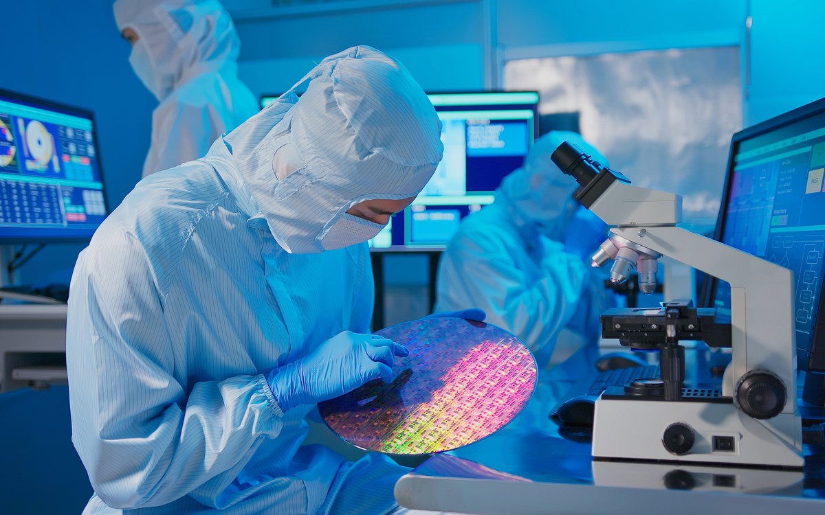
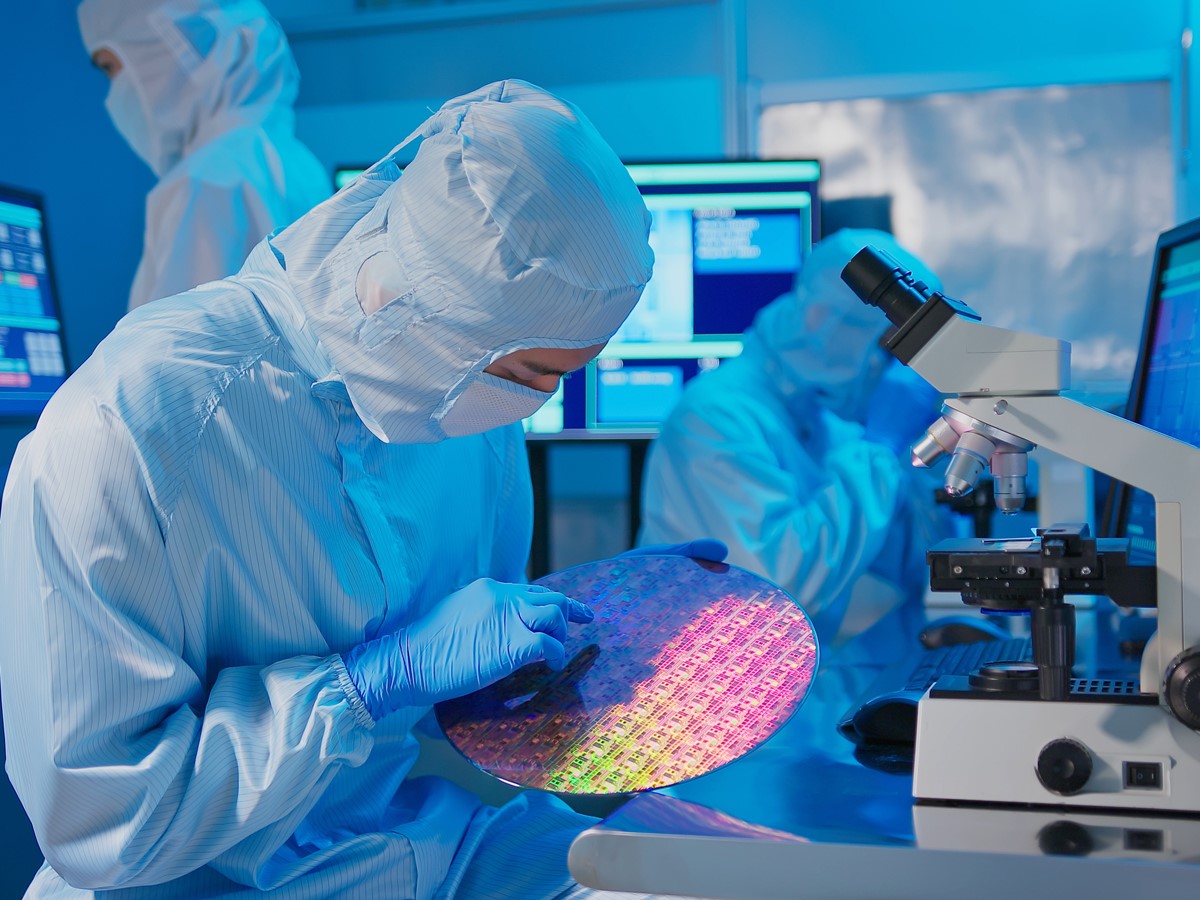
Semiconductor manufacturing relies on several advanced techniques to help create some highly efficient and durable electronic components. Plating processes are part of this, as they can form conductive layers that enhance electrical performance and reliability. Plating methods are used to deposit metal layers on semiconductor substrates, ensuring proper electrical connectivity, improved conductivity, and resistance to environmental degradation. In this article, we take a detailed look at the plating process used in semiconductor manufacturing and consider their importance and how they are applied.

Understanding plating processes in semiconductor manufacturing
Plating is a method of depositing metal films onto semiconductor wafers to create conductive pathways. It is these metal layers which facilitate the movement of electrical signals and help to provide crucial durability to the delicate structures within the microchips. The primary plating techniques which are used in semiconductor manufacturing include electroless plating and electroplating.
Electroplating
Electroplating is a commonly used process in which a metal layer is deposited onto a wafer through an electrochemical reaction. Initially, the semiconductor wafer needs to be cleaned to remove contaminants and ensure that there is a strong adhesion of the metal layer. Once this has been completed, the wafer is submerged in an electrolyte bath, which is a solution containing metal ions. Finally, an external current is applied, reducing the metal ions from the solution and depositing them onto the wafer surface.
The most common metals which are used in electroplating include copper, nickel, gold and silver. Generally, copper electroplating is considered vital for interconnects in integrated circuits (ICs) as it provides superior electrical conductivity and reliability.
Electroless plating
Electroless plating is different from electroplating since it does not require any external electrical current. It relies on auto-catalytic chemical reactions to deposit metal layers. The catalytic layer is first applied to the wafer to initiate the metal deposition, and then the wafer is immersed in a solution that contains metal ions and reducing agents. This is designed to help trigger the metal deposition. The reaction will continue until the desired metal thickness is achieved, allowing a process of controlled growth.
Electroless plating is often used for nickel and palladium deposition in semiconductor applications. Particularly for enhancing adhesion and preventing oxidation.
Importance of plating in semiconductor manufacturing
The reason that plating processes are so important in semiconductor manufacturing is down to their ability to create these high-quality conductive layers. The metal plating ensures that there is minimal resistance in interconnects, enhancing signal transmission in microchips and providing improved electrical conductivity. There is enhanced durability thanks to the plated layers which help to provide mechanical strength, corrosion resistance and an extended lifespan for semiconductor devices.
Plating is also important due to the precision and uniformity on offer. Advanced plating techniques can enable the deposition of ultra-thin uniform metal layers to ensure the high performance of semiconductor components. Plating is also vital for compatibility with different types of advanced technology. For example, it plays an important role in things like 3D integration, Microelectromechanical systems (MEMS) and next-generation semiconductor packaging.
The applications of plating in semiconductor manufacturing
-
Interconnect formation
Plating processes are most critically used in the formation of conductive layers for interconnects. In modern ICs, copper electroplating is favoured over traditional aluminium interconnects to reduce resistance and improve efficiency.
-
Wafer-level packaging (WLP)
Wafer level packaging relies on plating to help create redistribution layers (RDLs) and solder bumps. This enables efficient electrical connections between different chip components.
-
MEMS fabrication
MEMS devices tend to use a lot of electroless nickel plating as it helps to provide protective coatings that can enhance mechanical strength and resist environmental stress.
-
Advanced packaging technologies
Plating techniques help to form reliable electrical connections and facilitate high performance semiconductor packaging solutions in flip-chip bonding and through-silicon vias (TSVs).
The future of semiconductor plating
Plating processes have gradually been adapting alongside semiconductor technology advances to meet the continued demands for smaller and more powerful devices. This has led to innovations in nanoscale plating, and alternative metal deposition techniques to improve efficiency and performance. There are also new materials like cobalt and ruthenium, which are potential replacements for things like copper to help reduce electromigration and enhance reliability. In addition to this, there have been signs of advancements in environmentally friendly plating solutions which are focusing on reducing the number of hazardous chemicals involved and minimising semiconductor manufacturing waste.
Application specific requirements
Each industry and application will have its own unique requirements that will influence the choice of photoresist. Positive photoresists are better suited to advanced semiconductor manufacturing where miniaturisation and precision are critical, whilst negative photoresists are favoured in industries like printed circuit boards (PCB's) and packaging, where larger features and durability are the priority.
Semiconductor manufacturing relies on plating processes to provide essential conductive layers that can enhance the electrical performance and durability of a device. Whether it is through electroplating or electroless plating, these techniques have been designed to enable the precise deposition of metals that are critical for all our modern electrical devices. The evolution of the semiconductor industry is set to also bring about several advancements in plating technology, meaning that it will continue to play a pivotal role in the process.
