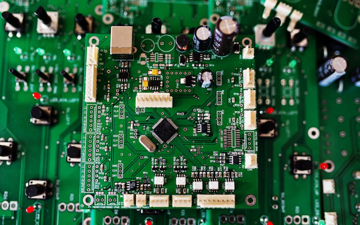
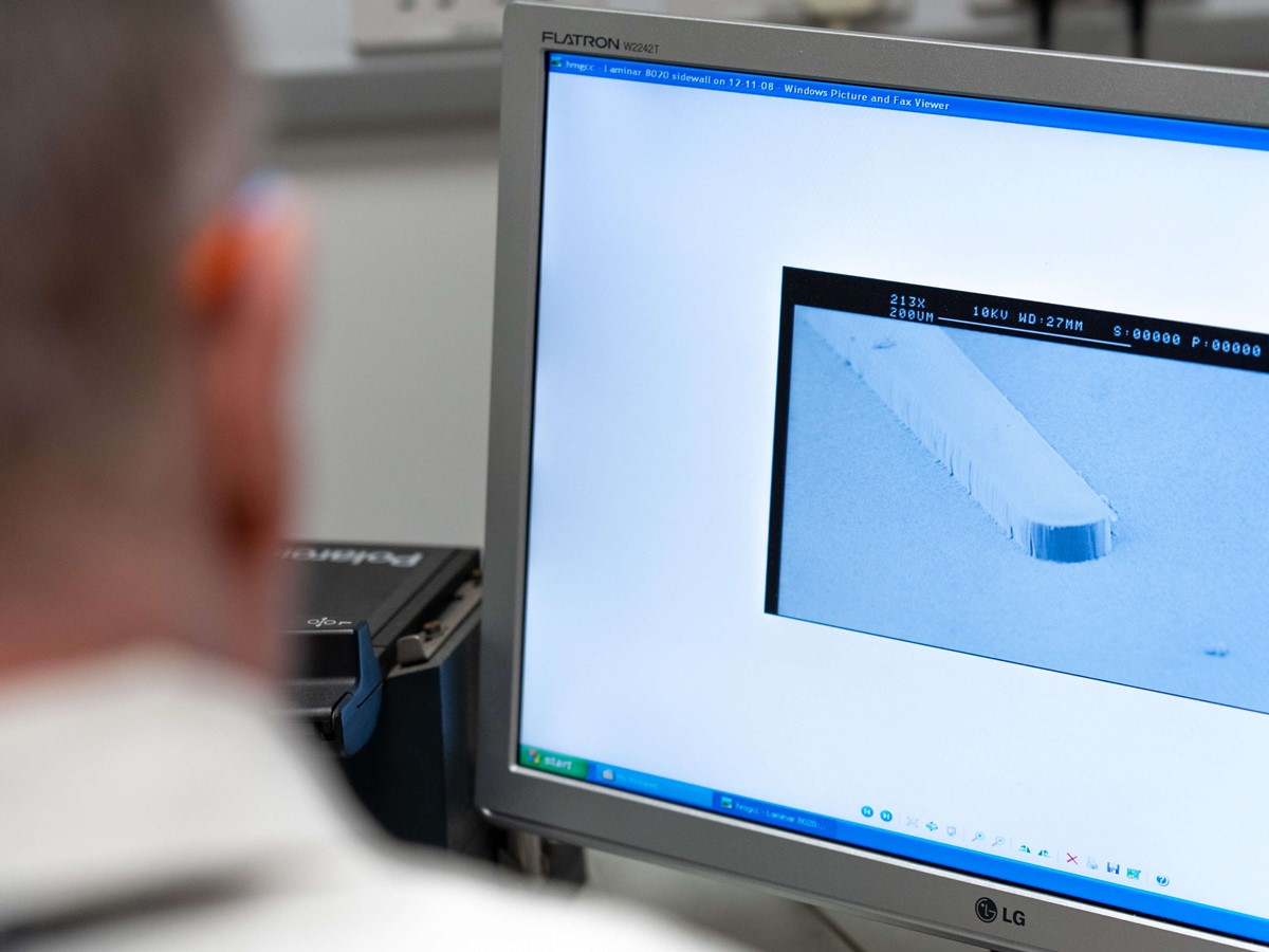
When developing a printed circuit board (PCB), you need to create a strong permanent layer that can both protect the copper traces and the interfaces between them. This is done using a photoimageable solder resist, which prevents any issues of conductive solder bridging between different components and causing short circuits. So, what are photoimageable solder resists and how can they help to enhance the precision of PCB manufacturing?

What is photoimageable solder resist?
A photoimageable solder resist, or a photoimageable solder mask (PSR) as it is sometimes known, is made up of different substances including things like epoxy resin, hardener, filler, dyes and UV-reactive substances. It is particularly important if reflow or solder bath processes are used as these do not allow for much control when molten solder bits land on the circuit board. Instead, photoimageable solder masks provide resistance and control in these situations, ensuring that the placement and movement of the solder is controlled.
Photoimageable solder masks are available in a range of different colours. Whilst the standard colours tend to be green and white, there are often also red, blue and black options depending on the use of the circuit board. In addition, there are a choice of finishes available including matt, semi-matt or gloss to support the use of optical inspection systems in production.
How does photoimageable solder resist work?
The main purpose of a photoimageable solder resist is to stop solder in its tracks and ensure the greatest levels of precision as part of PCB manufacturing. It creates bridges made of solder mask in between individual solder pads to prevent them from being short circuited to each other. They also create bridges between solder pads, component holes and vias to stop the solder from flowing uncontrollably from one side of the circuit board to another. In some cases, solder pads can be formed by selectively exposing copper surfaces from the solder mask.
The benefits
The main benefit of a photoimageable solder resist is to prevent short circuiting within any kind of circuit board component. This means the lifespan of the product can be increased, making it more reliable. It can also help to insulate individual conductors and protects against environmental influences which may cause corrosion. The photoimageable solder mask helps to prevent dirt and foreign material entering between the conductor traces, ensuring high quality and reliable functioning.
Photoimageable solder resist is particularly useful during the assembly stage of any printed circuit board. It ensures that only the areas which need to have a solder covering are soldered, ensuring much greater levels of precision during the soldering process. As many printed circuit boards have a very fine pitch it is very easy for small solder tracks to cause bridges and short circuits. The photoimageable solder masks ensure that solder is kept entirely to where it is meant to be, which allows the design of the circuit board to be enhanced, and more precise elements can be incorporated.
As electrical components become smaller and electrical connections within printed circuit boards become denser, then it is important for conventional solder masks to develop in order to meet new and more demanding requirements. This means that more advanced solder mask materials are now being created through the introduction of water-soluble groups, siloxane polymers, hyperbranched polymers, and reactive diluents to prevent some of the more common defects such as cracking and delamination.

