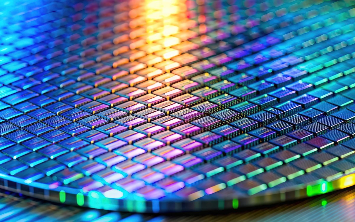
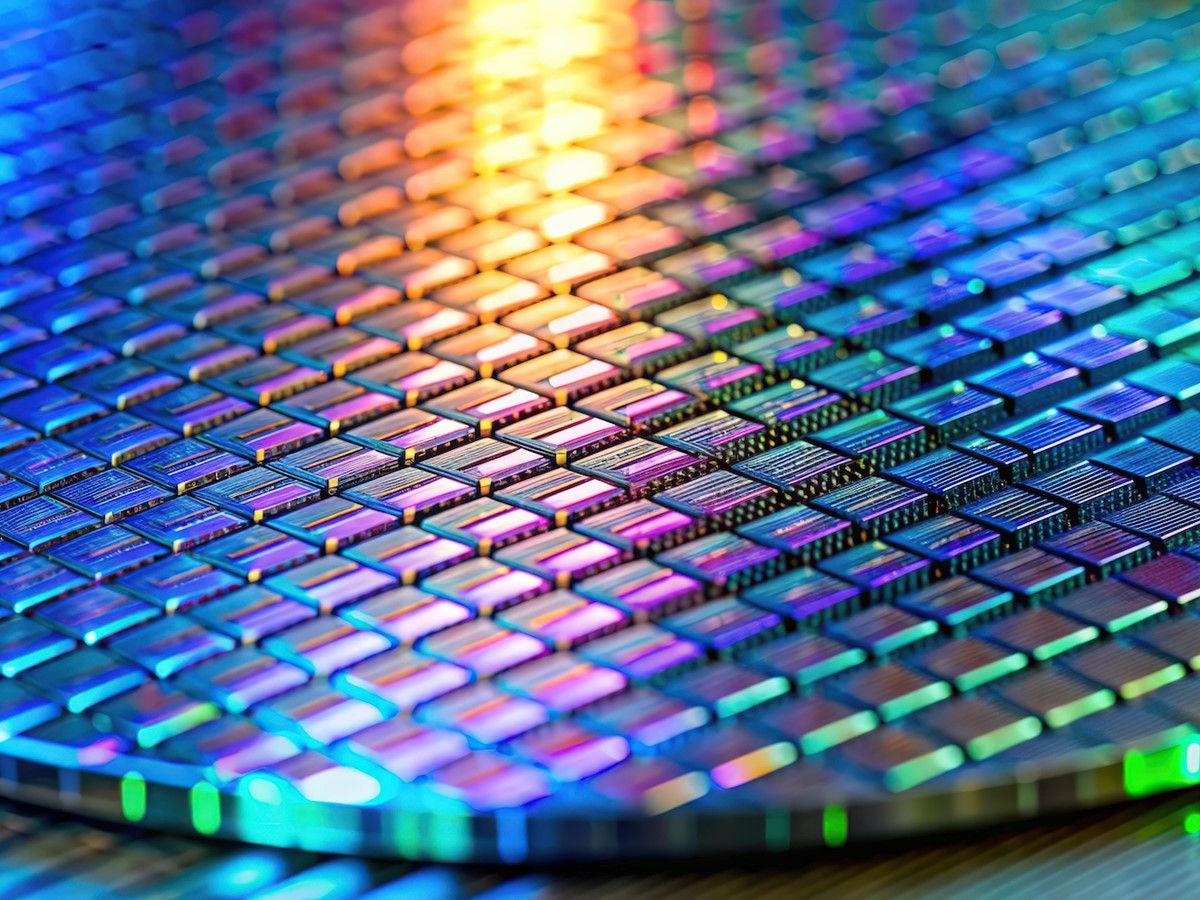
Semiconductor technology has come on in leaps and bounds over the last few years and this has driven the need for innovative materials and processes which can support increasingly complex packaging designs. As part of this, bonding adhesive photoresists have emerged as a crucial component in advanced packaging techniques. These materials play a pivotal role in ensuring precise alignment, structural integrity, and electrical performance in semiconductor devices. Here, we take a detailed look at bonding adhesive photoresists and their applications in advanced packaging.

Understanding bonding adhesive photoresists
Bonding adhesive photoresists are photosensitive materials that can serve as both an adhesive and a patternable resist layer in semiconductor processing. They can provide excellent adhesion as well as chemical resistance and mechanical stability, which makes them ideal for different advanced packaging techniques including wafer-level packaging (WLP), fan-out wafer-level packaging (FOWLP) and 3D integration.
Bonding adhesive photoresists have a number of unique properties which allow them to perform multiple functions within semiconductor fabrication. This includes providing structural support during wafer bonding and enabling fine-pitch lithography. In addition to this, they are capable of enhancing electrical connectivity through precise patterning and offering protection against environmental and mechanical stresses.
Applications in advanced packaging
-
Wafer-level packaging (WLP)
In wafer-level packaging, bonding adhesive photoresists are used to create high resolution patterns whilst ensuring mechanical stability during processing. Their ability to withstand thermal and chemical stresses makes them essential for fabricating interconnect structures that enhance semiconductor performance.
-
Fan-out wafer-level packaging (FOWLP)
FOWLP is an advanced semiconductor packaging technology that can improve electrical performance and reduces form factor. Bonding adhesive photoresists can facilitate the redistribution of interconnects and help to form multilayer structures, which enable more efficient power and signal transmission.
-
3D Integration and through silicon via (TSV) technology
With demand for compact and high-performance semiconductor devices continuing to grow, 3D integration has become a key focus area. Bonding adhesive photoresists support TSV fabrication by providing temporary adhesion for wafer bonding and enabling precise etching processes. These materials can then help to ensure reliable electrical connections between stacked dies, reducing signal delays and power consumption.
-
MEMS and sensor packaging
Microelectromechanical systems (MEMS) and sensor technologies rely on advanced packaging techniques to enhance device sensitivity and reliability. Bonding adhesive photoresists can provide critical support during sensor fabrication, protecting the delicate components while still enabling high resolution patterning and interconnect formation.
Advantages of bonding adhesive photoresists in semiconductor packaging
Bonding adhesive photoresists in advanced packaging have been integrated due to their high addition strength, they can help to ensure a robust mechanical stability during wafer bonding and post-processing steps. They also offer excellent chemical and thermal resistance as they can withstand harsh fabrication conditions, including exposure to solvents, etchants and high temperatures.
Bonding adhesive photoresists also support high resolution lithography which enables precise interconnect structures, and they can facilitate the formation of conductive pathways to minimise signal losses and improve power efficiency.
They are also compatible with multiple deposition, etching and bonding techniques, which makes them versatile for various semiconductor applications.
Future trends and innovations
Semiconductor packaging is continuing to advance and the demand for high performance bonding adhesive photoresist is expected to grow with it. Emerging trends include heterogeneous integration, where it becomes possible to combine different semiconductive technologies into a single package to help improve functionality and performance even further. The trend towards AI and high-performance computing (HPC) means that advanced packaging solutions will use bonding adhesive photoresists to enable faster and more efficient chip interconnects.
Flexible and wearable electronics are also becoming more popular, so it is essential to develop new adhesive photoresists that can support flexible substrates that allow the creation of next generation electronic devices. As the industry continues to explore eco-friendly bonding adhesive photoresists, it may become possible to reduce the environmental impact while still maintaining high performance standards.
It is clear that bonding adhesive photoresists are indispensable in advanced packaging as they play a critical role in enhancing semiconductor performance, reliability and miniaturisation. Their applications across wafer-level packaging, fan-out wafer-level packaging, 3D integration and MEMS fabrication only serves to highlight how versatile and important they have become as part of modern electronics. As the semiconductor industry continues to grow and evolve, innovations in bonding adhesive photoresists are likely to remain a key driver of progress shaping the future of advanced packaging solutions.
